If you’re a developer or are generally looking to acquire another valuable skillset that can complement coding, you might want to consider designing printed circuit boards (PCBs). Whether as a hobby or a new career pursuit, you’d be surprised how similar coding and PCB designing is. Similar to coding, PCB design can be easily learned and has a very smooth learning curve comparable to programming. Designing a PCB also follows the same logic, with a few key differences like the fact that PCBs are tested physically. But the process of developing a PCB and a program is largely the same. You progress from a design based on a logical flow and map out your functions to enable it to perform a task. As most PCBs today use software to create designs, having a coding background means you’re already halfway there.
What is a printed circuit board?
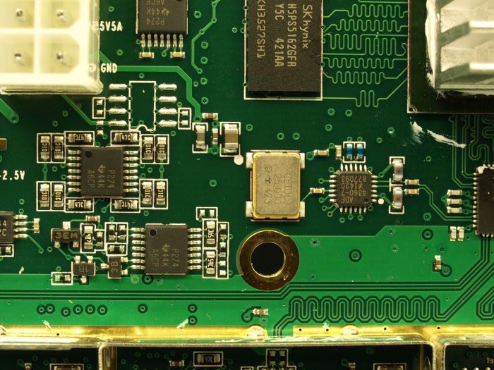
PCBs have basically made all of the modern electronics possible. In fact, before they were adopted in the latter half of the 20th century, connecting electrical components in any appliance often resulted in a huge tangle of wires. With the rise of PCBs, components and wires can now be neatly arranged and embedded in a more organized and flat board. PCBs embed these wires and components on a piece of fiberglass which also facilitates and controls the electric current that passes through it, which then enables its functions. The components vary depending on the complexity of the PCB design. But most include a combination of transistors, capacitors, inductors, transformers, and diodes, which are designed and placed depending on how the electricity passes through the system.
Creating a PCB
Slices of fiberglass are stacked together and coated with resin to make them stick to each other – making one solid slab. Then, layers of copper are applied to both sides and treated with a chemical called photoresist. After that, a pattern that matches exactly the components that are supposed to go on the board is placed on top. Then the whole thing is exposed to UV light. Afterward, the board is washed to remove the uncovered areas – leaving the tracks of copper. These copper patterns now serve as a base for how the PCB will ultimately look after other steps, including etching more copper. Boards are drilled with mounting holes to accommodate the components. Some of these holes also serve as tiny interconnectors between the different layers of copper traces. More advanced ones have cavities for bigger components like PCI express slots, heat sinks, and CPU sockets that are mounted or soldered onto the board. But because PCBs are just a collection of electrical connections on a substrate, you don’t need industrial tools or a whole factory to design one. With the design and prototyping tools available today, even startups and entrepreneurs can design their own PCBs for advanced electrical devices.
Designing a PCB is problem-solving
As mentioned above, you don’t have to have the expertise nor the upfront cost of factory floor prototyping in designing PCBs. Most of the PCBs that devices use today are designed digitally, prototyped, tested, and sent to third party manufacturers for scale production. Software used for PCB design follows design rules that enable makers to see if layouts, components, and requirements match. Like coding, designing a PCB means the first thing you have to solve is use-case. What is the purpose of your PCB? From there, there’s a wide array of software tools you can use to outline, populate and sequence your PCB with the components pertinent to the logic of its function. After creating the schematic of the design, you have to translate this into an actual circuit with dimensions, layers, traces, components, etc.
Prototyping and testing
After drafting the PCB layout, you can now create prototypes for testing. Prototyping can be an especially costly stage in creating PCBs and devices, and it typically costs an estimated $10,000. Similarly, testing a PCB can also be pricey – comprising 25% to 30% of the total product’s costs. This is why designing for testability in PCB design from the onset is a good way to save time and money when creating schematics. This also means knowing the capabilities of your manufacturer in testing coverage to minimize or eliminate defects before mass production. Similar to regression testing, you have to plan ahead so that your design enables you to test parts or features of the design in isolation so you won’t have to go through the entire system just to find out defects. In addition, testing PCBs also include testing its limits like identifying weak or brittle parts, determining states that demand more voltage, current and increase temperature, and if it can run for a long time. If all goes well, you can then start manufacturing or mass-producing your PCB – iteratively reducing costs and optimizing design as you get feedback. So, if you’re gunning for a spot in making today’s innovative electric devices possible, you should start learning how to make PCBs today.