Modern electronic devices are becoming smaller, faster, and more powerful with every new generation. From smartphones and laptops to advanced gaming systems, manufacturers are constantly pushing the limits of performance and design. One of the key technologies behind this evolution is Ball Grid Array (BGA) packaging.
Unlike older chip packaging methods that rely on pins around the edges, BGA uses a grid of tiny solder balls underneath the chip to create connections. This simple but powerful innovation allows engineers to design compact, high-performance devices without sacrificing reliability.
In this beginner-friendly guide, you’ll learn how BGA technology works, why it’s widely used in modern BGA electronics, and what makes it different from traditional packaging methods. By the end, you’ll have a clear understanding of why BGA plays such a crucial role in today’s electronics industry.
What is Ball Grid Array (BGA)?
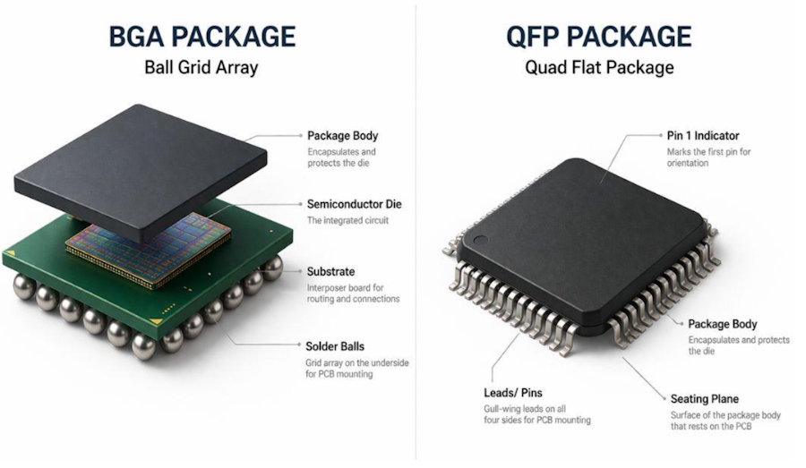
Ball Grid Array (BGA) is a type of surface-mount packaging used to connect integrated circuits to printed circuit boards (PCBs). Instead of metal leads or pins extending from the sides of the chip, BGA packages use an array of small solder balls arranged in a grid pattern on the underside.
These solder balls act as both electrical connections and mechanical support. When the chip is mounted on a PCB and heated during soldering, the balls melt, forming secure connections with the corresponding pads on the board.
This design offers a major advantage over older packaging types. By placing connections underneath the chip instead of around its edges, BGA allows for significantly more connection points in a smaller area. That’s one of the main reasons it has become a standard in modern electronics.
How BGA Technology Works
To understand how BGA works, it helps to look at the process from assembly to final connection. Although it may sound complex, the concept is quite straightforward when broken down.
The process begins with the semiconductor chip, also known as the die, being mounted onto a substrate. This substrate acts as an intermediary layer that routes electrical signals between the chip and the solder balls.
Once the chip is attached, tiny solder balls are placed on the underside of the package in a precise grid layout. Each ball corresponds to a specific electrical connection. The spacing and arrangement are carefully designed to match the PCB layout.
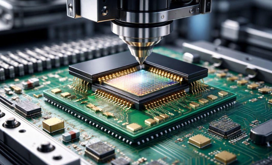
During assembly, the BGA package is positioned on the PCB so that each solder ball aligns perfectly with its corresponding pad. The board then undergoes reflow soldering, in which it is heated in a controlled environment. As the temperature rises, the solder balls melt, forming strong electrical and mechanical bonds with the PCB.
After cooling, the solder solidifies, forming a permanent connection. The result is a compact, highly reliable interface between the chip and the board, capable of supporting high-speed signals and efficient power delivery.
This process is a core reason why BGA electronics are widely used in advanced devices where precision and performance are critical.
Inside a BGA Package
A BGA package may look simple from the outside, but internally it is made up of several layers that work together to ensure performance and durability.
At the center is the semiconductor die, which performs the actual processing tasks. This die is mounted on a substrate that acts as a bridge between the chip and the external connections. The substrate contains tiny conductive traces that route signals efficiently.
Underneath the substrate, the solder balls form the connection interface with the PCB. These balls are carefully sized and spaced to ensure proper alignment and reliable solder joints.
The entire structure is protected by an encapsulation layer that shields the delicate components from environmental damage, such as moisture and dust. At the same time, the design allows heat to dissipate effectively, which is essential for high-performance applications.
Advantages of BGA Technology
One of the main reasons BGA has become so popular is its ability to support modern electronic demands without increasing size. By placing connections beneath the chip, BGA enables a much higher number of connections than traditional packages.
This higher connection density translates directly into better performance. Signals can travel shorter distances, which improves speed and reduces interference. At the same time, the compact design helps manufacturers create smaller and more efficient devices.
Another important advantage is thermal performance. Because the solder balls are spread across the underside of the package, heat can dissipate more evenly. This reduces the risk of overheating and improves the overall reliability of the device.
Mechanical reliability is also improved. The solder joints in a BGA package are generally stronger and less prone to damage compared to thin leads found in older packaging types.
Limitations and Challenges of BGA
Despite its many advantages, BGA technology is not without its challenges. One of the biggest issues is inspection. Since the solder joints are hidden underneath the chip, it is difficult to visually inspect them after assembly. Specialized equipment, such as X-ray inspection, is often required to detect defects.
Repair and rework can also be more complex. Removing and replacing a BGA chip requires precise temperature control and advanced tools. This makes the process more expensive and time-consuming compared to other package types.
Another challenge is manufacturing precision. Even a slight misalignment during assembly can lead to connection failures. That’s why high-quality assembly processes are essential when working with BGA components.
Companies like TSTRONIC focus on maintaining strict quality control standards to ensure reliable results in BGA electronics manufacturing. This level of expertise is critical for minimizing defects and ensuring consistent performance.
BGA vs Traditional Packaging Methods
To fully appreciate BGA technology, it helps to compare it with older packaging types such as Quad Flat Package (QFP) and Dual Inline Package (DIP).
Traditional packages rely on pins that extend from the sides of the chip. While this makes them easier to inspect and repair, it also limits the number of connections that can be achieved within a given space. As a result, they are not suitable for high-density, high-performance applications.
BGA, on the other hand, uses the entire underside of the chip for connections. This allows for a much higher pin count and better electrical performance. However, it comes at the cost of increased complexity in manufacturing and inspection.
In modern electronics, where performance and miniaturization are top priorities, BGA has become the preferred choice.
Comparison Table
|
Feature |
BGA (Ball Grid Array) |
QFP (Quad Flat Package) |
DIP (Dual Inline Package) |
|
Connection Method |
Solder balls underneath |
Leads on sides |
Pins through holes |
|
Package Size |
Very compact |
Medium |
Large |
|
Pin Density |
Very high |
Moderate |
Low |
|
Electrical Performance |
Excellent (high-speed) |
Good |
Limited |
|
Heat Dissipation |
Excellent |
Moderate |
Poor |
|
Inspection |
Difficult (hidden joints) |
Easy |
Very easy |
|
Rework & Repair |
Complex |
Moderate |
Easy |
|
Common Applications |
CPUs, GPUs, smartphones |
Microcontrollers |
Basic circuits |
Where BGA is Used in Modern Electronics
BGA technology is now widely used across a range of electronic devices. It is especially common in products that require high processing power and compact design.
You’ll find BGA packages in smartphones, laptops, graphics cards, gaming consoles, and even automotive electronics. These applications benefit from the high connection density and improved thermal performance that BGA provides.
As devices continue to become more advanced, the role of BGA in electronics is only expected to grow.
Common BGA Assembly Issues
Although BGA is highly reliable, certain issues can arise during assembly if not handled correctly. Problems such as solder bridging, voids within solder joints, and misalignment can affect performance and durability.
These issues are often caused by improper temperature control, inaccurate placement, or poor-quality materials. That’s why precision and expertise are essential in BGA assembly.
Working with experienced manufacturers like TSTRONIC helps reduce these risks by ensuring proper process control and consistent quality throughout production.
Simple Way to Understand BGA (Beginner Tip)
If you’re new to this topic, a helpful way to think about BGA is to imagine a grid of tiny connection points hidden underneath a chip. Instead of wires or pins sticking out, everything is neatly arranged below the surface.
This hidden grid allows the chip to connect more efficiently while saving space, which is exactly what modern electronics need.
Conclusion
Ball Grid Array (BGA) technology has become a cornerstone of modern electronics, enabling the development of smaller, faster, and more powerful devices. By replacing traditional pins with a grid of solder balls, BGA offers higher connection density, better performance, and improved thermal management.
While it does come with challenges such as inspection and rework complexity, its advantages far outweigh the limitations in most applications. That’s why it is widely used in today’s high-performance devices and continues to play a critical role in the evolution of bga electronics.
As technology advances, the demand for compact and efficient designs will only increase, making BGA even more important in the future. With the right expertise and quality standards, companies like TSTRONIC are helping drive innovation and reliability in this rapidly evolving field.
FAQ
1. What is Ball Grid Array (BGA) in electronics?
Ball Grid Array (BGA) is a surface-mount packaging technology that uses tiny solder balls under a chip to connect it to a PCB. It enables higher connection density and better performance than traditional packages.
2. Why is BGA used in modern electronics?
BGA is used because it enables compact design, high-speed performance, and efficient heat dissipation, making it ideal for devices such as smartphones, laptops, and GPUs.
3. How are BGA chips soldered onto a PCB?
BGA chips are soldered using a reflow process, in which heat melts the solder balls beneath the chip, forming strong electrical and mechanical connections to the PCB.
4. What are the main advantages of BGA technology?
The main advantages include higher pin density, better electrical performance, improved thermal management, and smaller package size.
5. Can BGA components be repaired or reworked?
Yes, but BGA rework is complex and requires specialized equipment and expertise due to the hidden solder joints beneath the chip.