
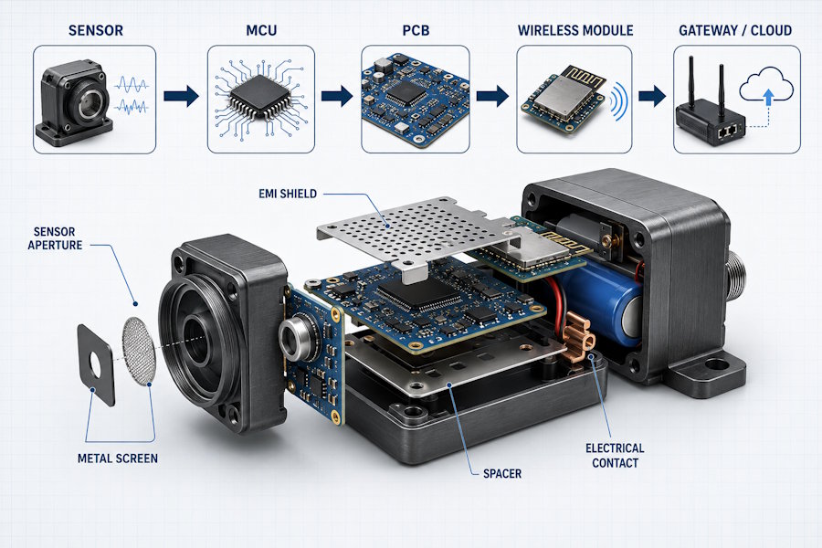
A working PCB does not automatically mean a reliable IoT product. Firmware may run correctly, sensors may return data, and wireless connections may work during testing. But once the electronics are placed inside a real enclosure, problems with interference, alignment, airflow, spacing, and electrical contact can appear. This is why manufacturing methods such as photochemical etching matter when developers move from a prototype board to a complete physical device.
IoT Hardware Is More Than a PCB
An IoT device normally combines several systems. It may contain a microcontroller, sensors, wireless modules, power circuits, antennas, connectors, and a PCB.
These electronics must then fit inside an enclosure and interact with the real world. A temperature sensor needs exposure to the environment. An optical sensor may need a precisely positioned opening. A wireless module must operate without unnecessary interference.
This means mechanical and electrical details become part of product performance.
Developers who focus only on firmware and PCB design may discover these problems late in the project, when changing the enclosure or hardware becomes more expensive.
Precision Components Developers Often Overlook
Many IoT products contain small metal parts that receive little attention during early software development. Their functions can still be important.
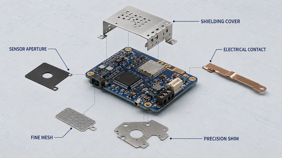
Sensor Apertures and Plates
Sensors often need controlled access to light, air, sound, or other environmental inputs.
A metal sensor plate can contain small holes, slots, or apertures that define what reaches the sensor. The position of these openings must match the PCB, sensor, and enclosure.
Optical devices may require even more precise alignment. A small change in an aperture or mounting position can affect how the sensor receives information.
Shims and Spacers
Shims and spacers control gaps and assembly height.
They may position a sensor above a PCB, maintain a gap between modules, align an enclosure component, or adjust the position of a mechanical interface.
These parts are often simple, but their thickness can influence the final assembly. A device that works on a development bench may behave differently when every component is packed into a compact housing.
Fine Metal Screens
IoT devices often need openings for airflow, sound, sensing, or pressure measurement. These openings can also allow dust or larger particles to enter.
Fine metal screens provide a physical barrier while maintaining an open area for air or other signals to pass through.
The hole size, pattern, open area, material, and outer profile can all be adjusted for the application.
EMI Becomes a Bigger Issue in Compact Devices
Modern IoT products often place wireless communication, processors, power electronics, sensors, and antennas close together.
These components can generate electromagnetic noise or be affected by interference from nearby circuits.
EMI shielding can help protect selected areas of a PCB or reduce emissions from a noise source. A thin shielding cover may contain ventilation holes, mounting feet, grounding contacts, identification marks, and bend lines.
However, adding a metal cover alone does not guarantee good electromagnetic compatibility. Grounding, seams, openings, antenna position, material, and the PCB layout must all be considered together.
How Photochemical Etching Works
Photochemical etching, also called photo etching or chemical etching, produces flat metal components by selectively removing material from a metal sheet.
The process starts by cleaning the sheet and applying a light-sensitive photoresist. Digital artwork defines the part geometry. Ultraviolet exposure transfers that pattern onto the coated metal.
After development, an etchant removes the unprotected areas. The remaining parts are then stripped, cleaned, and inspected.
The process can create holes, slots, grids, apertures, tabs, outer profiles, identification marks, and other features in the same flat component.
Because a cutting tool does not press directly against the sheet, the process avoids direct mechanical cutting force on thin metal.
Why Etching Fits IoT Product Development
IoT hardware often changes several times before production.
A sensor may move after field testing. A shielding cover may need a larger ventilation area. A spacer may require another opening. A screen pattern may need to balance protection and airflow differently.
Photochemical etching uses digital artwork instead of a dedicated cutting tool or hard stamping die. Engineers can therefore modify the pattern when the component design changes.
This makes the process useful for prototypes, engineering validation, pilot builds, and selected repeat-production programs.
It is especially suitable for thin flat parts that contain many detailed features.
For example, a sensor plate can include its aperture, mounting holes, alignment features, and outer profile in one design. A shielding blank can include ventilation patterns, mounting tabs, and fold lines before it is formed into its final shape.
From Code to Real Hardware
IoT development can be viewed as a chain:
Code → MCU → PCB → Sensors → Precision Components → Enclosure → Real-World Device
A problem at any stage can affect the final product.
Software may process sensor data perfectly, but poor sensor alignment can still produce unreliable input. A wireless protocol may work correctly, while poor shielding or grounding creates unwanted interference. A PCB may meet its dimensions, while an incorrect spacer prevents the enclosure from closing properly.
For this reason, hardware manufacturability should be considered before the design is frozen.
Developers should review component thickness, tolerance, mounting method, environmental exposure, electrical requirements, and later assembly steps during prototype development.
Where These Components Appear
The same design principles can apply across many IoT products.
Smart home devices may use screens, contacts, sensor openings, and shielding around wireless electronics. Industrial IoT systems may require durable sensor plates, filters, spacers, and grounding components.
Environmental monitoring devices can use fine screens and apertures to expose sensors while providing physical protection. Edge devices may need shielding and thermal-management components around processors and communication modules.
The exact solution depends on the device rather than the IoT label itself.
When Other Manufacturing Methods Make More Sense
Photochemical etching is not the best manufacturing process for every component.
CNC machining is more suitable for many thick or three-dimensional parts. Stamping can offer lower unit costs for simple components produced in very high volumes. Laser cutting can work well for many thicker flat parts.
Etching becomes more attractive when the component is thin, flat, detailed, or likely to change during product development.
Material, thickness, tolerance, geometry, volume, forming, plating, inspection, and total cost should all be considered before selecting a process.
Design for the Complete Device
IoT development does not end when the firmware compiles or the PCB passes a bench test.
A reliable product depends on how software, electronics, sensors, communications, mechanical parts, and the enclosure work together.
When teams need thin metal parts with detailed openings, grids, tabs, contacts, or alignment features, a qualified metal etching supplier can review the design alongside material, thickness, tolerances, forming, finishing, and production requirements.
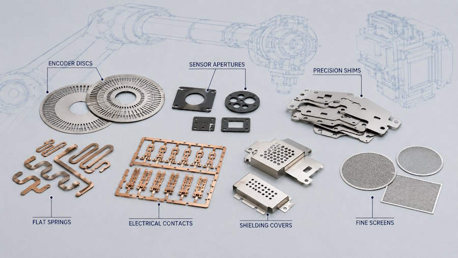
Precision components may represent only a small part of an IoT device, but they connect digital design with the physical world. Considering them early can make the move from prototype to finished hardware more predictable.